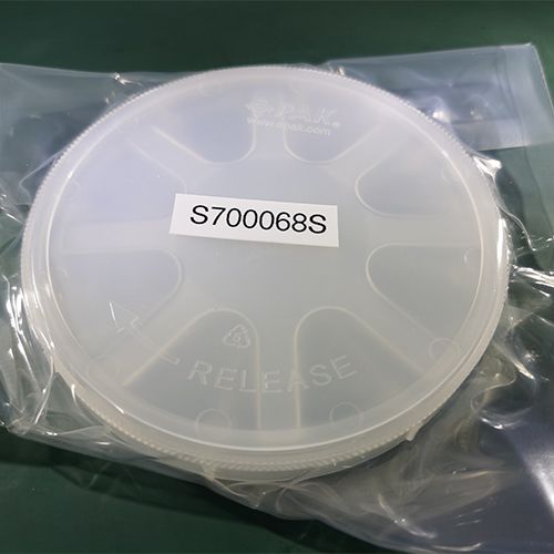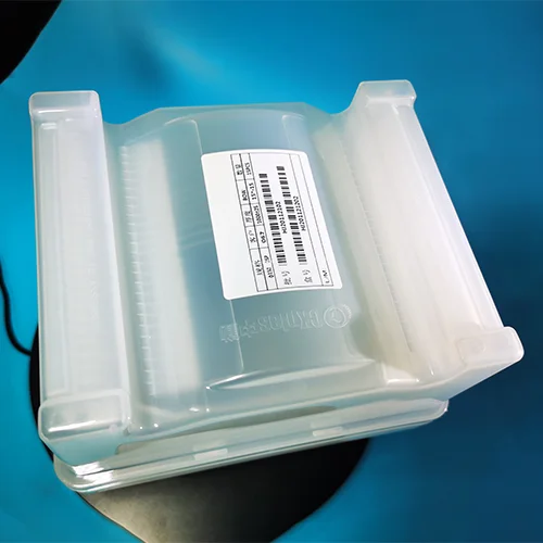
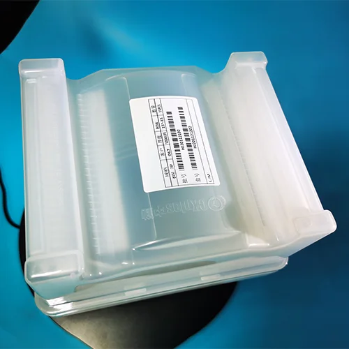
2-inch silicon wafers for research, process development and drawing-led semiconductor enquiries. Local quotation material records N-type low-resistivity and intrinsic 2-inch options; final grade, oxide and thickness must be confirmed per order.
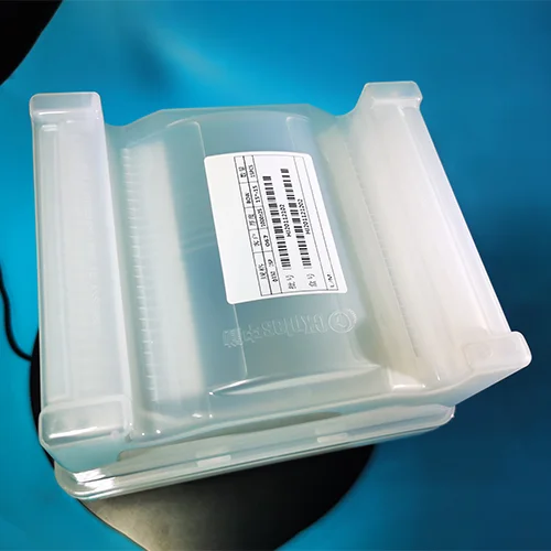
Product Description
2-inch silicon wafers for research, process development and drawing-led semiconductor enquiries. Local quotation material records N-type low-resistivity and intrinsic 2-inch options; final grade, oxide and thickness must be confirmed per order. Final grade, tolerances and acceptance criteria require quotation review.
Applications
Research and teaching
A compact wafer format for laboratory process trials and device-structure experiments.
Semiconductor process development
Useful when a buyer needs a controlled substrate size for deposition, lithography or etch development.
Oxide-interface studies
An oxide-bearing option can be evaluated when the interface thickness and measurement method are defined.
Prototype device work
Specify orientation, resistivity, polish and cleaning requirements before committing the wafer to a process flow.
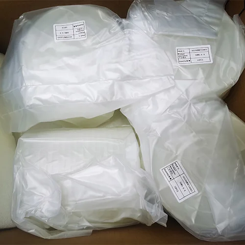
Specification and Acceptance Checklist
| Diameter | 2 inch |
|---|---|
| Material options | N-type low-resistivity silicon; intrinsic silicon option |
| Resistivity | Low-resistivity option recorded as <0.01; verify test basis and lot |
| Oxide | No oxide option; 300 nm oxide option recorded for intrinsic silicon |
| Thickness | 500 µm recorded in local quotation material |
| Polish | Single-side polish recorded for low-resistivity option |
| Use | Research, process development and semiconductor prototyping |
| Orientation | Specify crystal orientation in the RFQ |
| Doping | Specify conductivity type and dopant requirement |
| Acceptance | Confirm inspection, packing and traceability before order |
RFQ Information
- Diameter and usable area
- Conductivity type and dopant
- Resistivity range and test method
- Crystal orientation and off-axis angle
- Native oxide or specified oxide thickness
- Thickness and tolerance
- Single-side or double-side polish
- Surface quality, particles and bow/warp
- Quantity, packing and traceability
- Destination and required delivery date
Procurement FAQs
What size silicon wafers are described here?
The local quotation material records a 2-inch wafer option. Confirm the actual diameter standard and usable area in the order.
Are these wafers N-type?
An N-type low-resistivity option is recorded. Conductivity type and dopant must be confirmed for each quotation.
Is resistivity guaranteed below 0.01?
The local quotation material records a low-resistivity option below 0.01, but the test basis and lot acceptance must be confirmed.
Can I request an oxide layer?
Yes, a 300 nm oxide option is recorded for intrinsic silicon material; confirm thickness measurement and uniformity requirements.
What thickness is listed?
500 µm is recorded in the local quotation material. Tolerance and measurement method remain order-specific.
Are the wafers polished?
A single-side polish is recorded for the low-resistivity option. Specify the required polish and surface acceptance.
Can you supply a different orientation?
Orientation should be stated on the drawing or RFQ. Feasibility must be confirmed for the requested material and size.
Are these production-qualified wafers?
This page describes quotation options, not a blanket production qualification. Request lot records and acceptance data for the application.
How should wafers be packed?
State single-wafer or cassette packing, cleanliness, labeling and traceability requirements in the RFQ.
How are price and lead time determined?
They depend on grade, oxide, polish, inspection, quantity and destination and require an order-specific quotation.
Xinkehui Project Support
Shanghai Xinkehui New Materials Co., Ltd. describes engineering, precision processing and inspection capabilities in its public company materials. The applicable process, test and delivery scope must be confirmed for the selected material and order.
Contact Xinkehui with the drawing, operating conditions and RFQ details above.