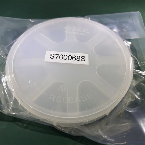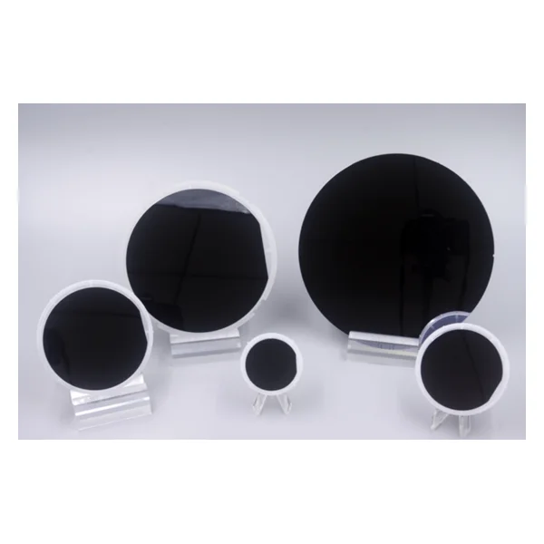
Gallium arsenide wafers for RF, optoelectronic and semiconductor research enquiries. Specify orientation, conductivity, diameter, thickness, polish, surface criteria and packaging in a controlled RFQ.
Product Description
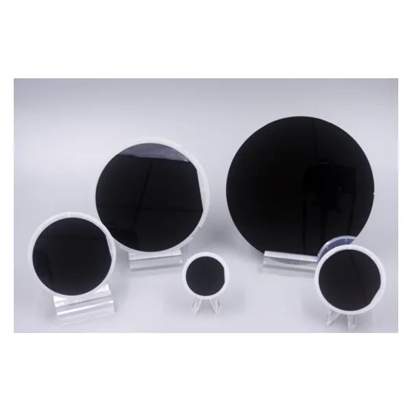
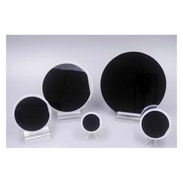
Gallium arsenide wafers for RF, optoelectronic and semiconductor research enquiries. Specify orientation, conductivity, diameter, thickness, polish, surface criteria and packaging in a controlled RFQ. Final grade, dimensions and acceptance criteria require quotation review.
Product Applications
RF and microwave research
GaAs substrates may be evaluated for high-frequency device experiments when orientation, conductivity and surface acceptance are defined.
Optoelectronic development
Use the actual device wavelength, epitaxy or deposition flow and surface requirements to determine substrate suitability.
Semiconductor process trials
Specify diameter, thickness, polish, bow/warp and cleanliness for repeatable laboratory process work.
Prototype and teaching devices
A drawing-led enquiry helps align wafer format, material grade, inspection and packing with the experiment.
Specification and Acceptance Checklist
| Material | Gallium arsenide (GaAs); grade to be confirmed |
|---|---|
| Wafer function | Semiconductor research substrate |
| Diameter | Specify nominal diameter and usable area |
| Orientation | Crystal orientation and off-axis angle |
| Conductivity | Semi-insulating or conductive requirement to be stated |
| Thickness | Nominal thickness and tolerance |
| Polish | Single-side or double-side polish |
| Surface | Particles, defects, roughness and edge criteria |
| Electrical acceptance | Resistivity or carrier criteria and test method |
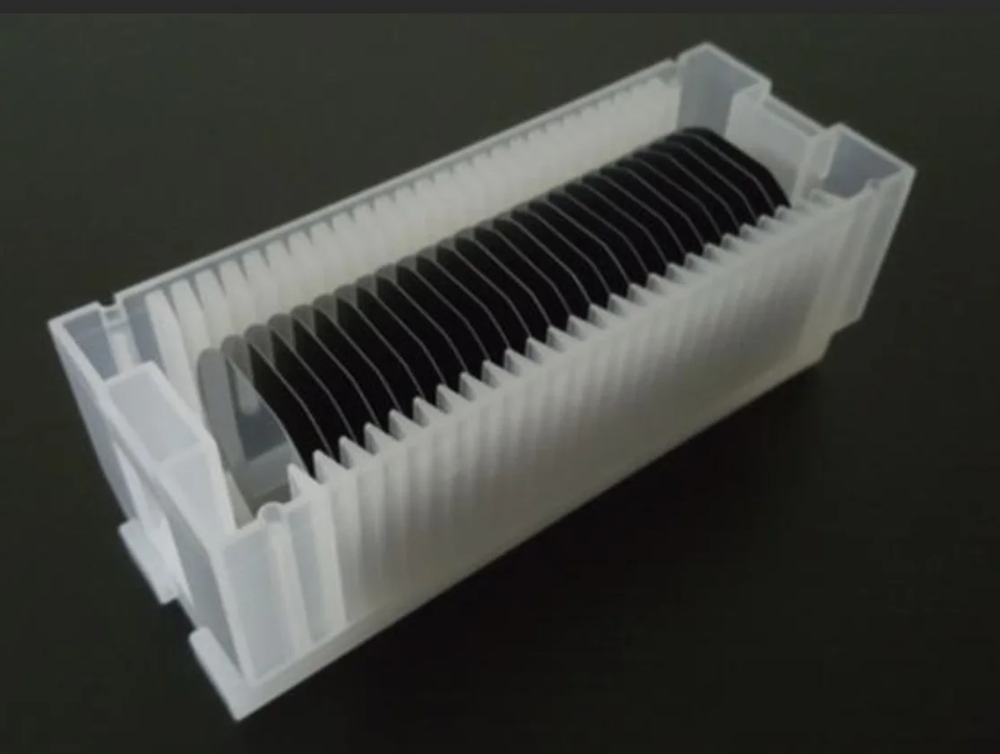
| Packing | Cassette or single-wafer container and labeling |
RFQ: 10 Information Items
- GaAs grade and intended device process
- Diameter and usable area
- Crystal orientation and off-axis angle
- Conductivity or semi-insulating requirement
- Resistivity and test method
- Thickness and tolerance
- Single-side or double-side polish
- Surface, particles, bow and warp criteria
- Packing, labeling and traceability
- Quantity, destination and requested delivery date
Ten Procurement FAQs
1. What are GaAs wafers used for?
They may be evaluated for RF, microwave, optoelectronic and semiconductor research applications.
2. Are these wafers production-qualified?
This page is a procurement guide, not a blanket production qualification; request lot-specific acceptance data.
3. Can I specify semi-insulating GaAs?
Yes, state semi-insulating or conductive material and the required electrical test method in the RFQ.
4. Which orientation should I request?
Provide the device process orientation and any off-axis angle; feasibility is order-specific.
5. Can thickness be customized?
State nominal thickness and tolerance on a controlled drawing for review.
6. Is double-side polish available?
Specify single-side or double-side polish; the applicable option must be confirmed for the selected grade.
7. What surface checks matter?
Define particles, scratches, roughness, bow, warp and edge requirements relevant to the process.
8. How are wafers packed?
State cassette or single-wafer packing, labeling and cleanliness requirements.
9. Can you provide electrical test data?
Request resistivity or carrier data and the test basis required for acceptance.
10. How are price and delivery determined?
They depend on grade, size, electrical criteria, inspection, quantity and destination and require quotation.
Xinkehui Company Capability
Shanghai Xinkehui New Materials Co., Ltd. describes engineering, precision processing and inspection capabilities in its public company materials. Applicable processing, tests, packaging and delivery terms must be confirmed for the selected material and order.
Send a drawing, operating conditions and the RFQ details above for an order-specific review. This page does not assert price, stock, certification or delivery promises.