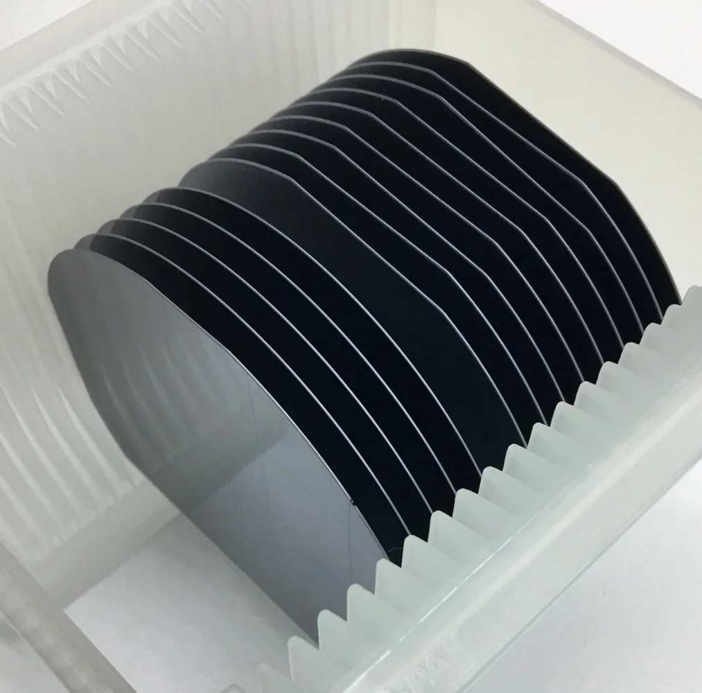
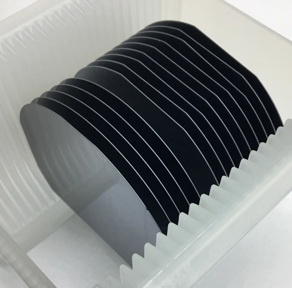
P-type 4H-SiC and 6H-SiC substrate options for power, high-temperature and high-frequency device development. The local 2024 specification document defines diameter, thickness, off-axis, grade, polish and inspection fields; confirm the exact grade and lot before purchase.
Product Description
P-type 4H-SiC and 6H-SiC substrate options for power, high-temperature and high-frequency device development. The local 2024 specification document defines diameter, thickness, off-axis, grade, polish and inspection fields; confirm the exact grade and lot before purchase. Final grade, tolerances and acceptance criteria require quotation review.
Applications
Power semiconductor development
A wide-bandgap substrate option for device process development where polytype, conductivity and defect criteria are controlled.
High-temperature electronics
The material family can be evaluated for elevated-temperature research, subject to device design and lot qualification.
High-frequency and optoelectronic work
The specification document lists high-frequency and optoelectronic device applications; confirm the exact process fit.
Epitaxy preparation
CMP, orientation, thickness and surface-defect acceptance should be aligned with the epitaxy or deposition process.

Specification and Acceptance Checklist
| Polytype | 4H-SiC or 6H-SiC |
|---|---|
| Conductivity | P-type; aluminum is listed as the dopant code |
| Diameter options | 2 inch, 4 inch and 6 inch classes are defined in the specification document |
| Thickness | 350 µm nominal options are listed; tolerance is grade and diameter dependent |
| Orientation | Off-axis 2°–4° toward the specified direction is listed for 4H/6H-P |
| Grades | Zero MPD production, standard production and dummy grades |
| Surface | Polish or CMP; roughness limits depend on grade |
| Inspection | Micropipe, polytype, scratches, edge chips, bow, warp and TTV fields are defined |
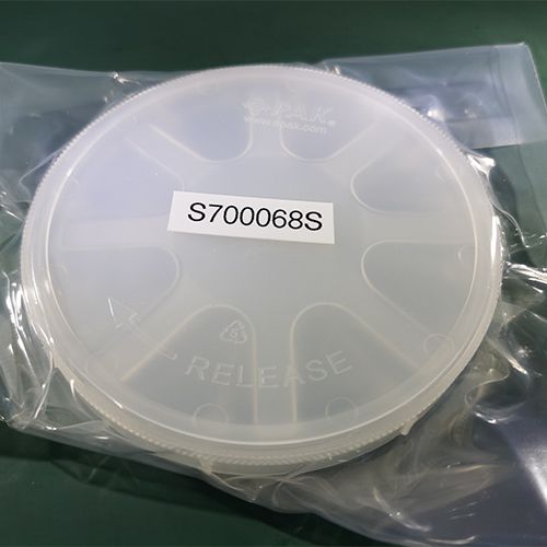
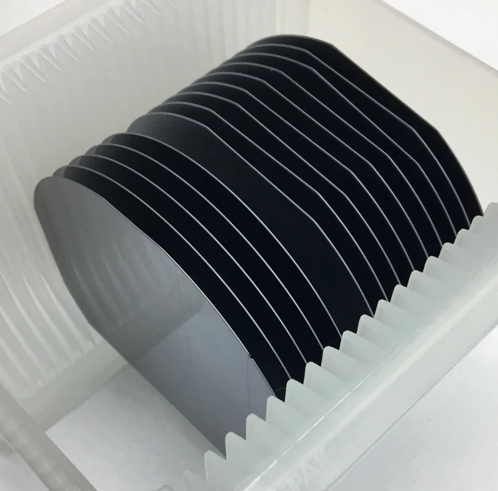
| Packaging | Multi-wafer cassette or single-wafer container |
| Acceptance | Use the current controlled specification and lot inspection plan |
RFQ Information
- Polytype: 4H or 6H
- P-type dopant and resistivity requirement
- Diameter and usable aperture
- On-axis or off-axis angle and direction
- Thickness and TTV/bow/warp limits
- Zero MPD, production or dummy grade
- Polish or CMP and roughness
- Micropipe, polytype and surface-defect limits
- Packing, labeling and traceability
- Quantity, destination and required delivery date
Procurement FAQs
Which polytypes are covered?
The local specification covers P-type 4H-SiC and 6H-SiC, with separate 3C-N material references. Request the exact polytype in the RFQ.
What dopant is associated with P-type material?
The specification coding lists aluminum as the P-type dopant. Confirm the required resistivity and measurement method.
What diameters are available?
The specification defines 2-inch, 4-inch and 6-inch diameter classes. Confirm current feasibility for the selected grade.
What thickness is listed?
350 µm nominal is listed in the local tables, with tolerances depending on diameter and grade.
Can I request an off-axis wafer?
Yes. The document lists off-axis ranges for 4H/6H-P; state angle, direction and tolerance explicitly.
What is Zero MPD grade?
It is a production-grade category identified in the source specification. Acceptance must be verified with the lot inspection plan.
Is CMP available?
CMP is listed as a surface option. Confirm roughness, flatness and inspection records for the requested lot.
What defects are inspected?
The document defines fields for micropipes, polytype areas, scratches, edge chips, bow, warp and TTV, among others.
How are wafers packed?
The source specification lists multi-wafer cassette or single-wafer container. State the required packing and labeling system.
Can you guarantee device performance?
No. This page describes substrate procurement criteria; device performance requires application-specific process and lot qualification.
Xinkehui Project Support
Shanghai Xinkehui New Materials Co., Ltd. describes engineering, precision processing and inspection capabilities in its public company materials. The applicable process, test and delivery scope must be confirmed for the selected material and order.
Contact Xinkehui with the drawing, operating conditions and RFQ details above.