1/1
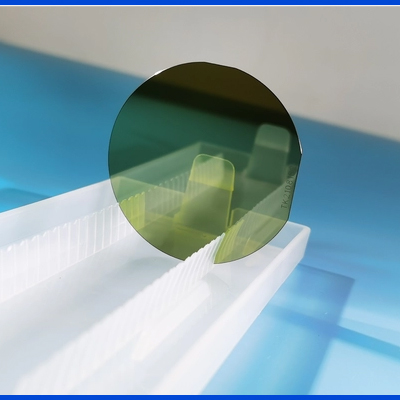
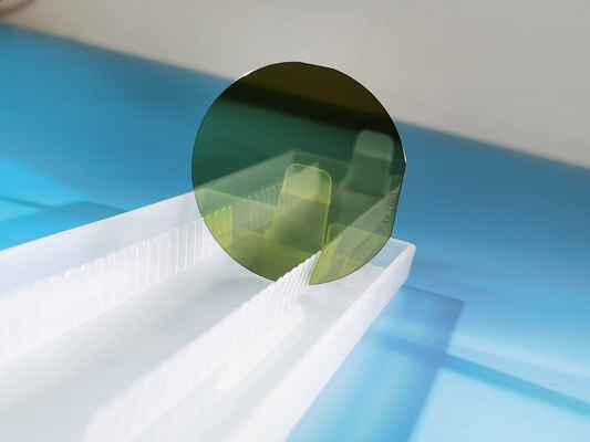
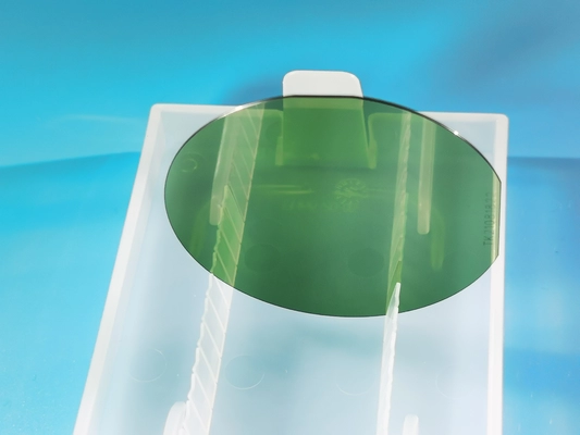
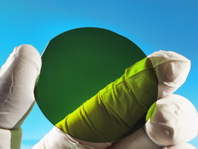
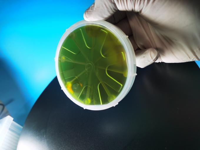
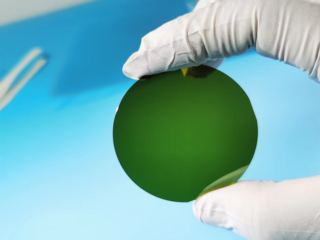
High quality factory price SIC wafer type 4H-N for MOS devices 2 “diameter 50.6mm
High quality factory price SIC wafer type 4H-N for MOS devices 2 “diameter 50.6mm
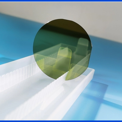
High quality factory price SIC wafer type 4H-N for MOS devices 2 “diameter 50.6mm
High quality factory price SIC wafer type 4H-N for MOS devices 2 “diameter 50.6mm
Shanghai Xinkehui Material Tech. Co., Ltd produces wafers to all SEMI Standards including dimensional, flat, and notch specifications. In addition, we offer customspecifications designed to your unique needs including, alignment marks, holes, pockets, edge profile, thickness, flatness,
surface quality, cleanliness, or any other details critical to your application. We also offer these wafers in a broad array ofmaterials including Borosilicate, Aluminosilicate, Fused Silica (instead of quartz), Quartz, and Soda Lime.
| Place of Origin: | CHINA |
| Brand Name: | xkh |
| Model Number: | 2inch SiC wafers |
| Minimum Order Quantity: | 25pcs |
|---|---|
| Price: | by case |
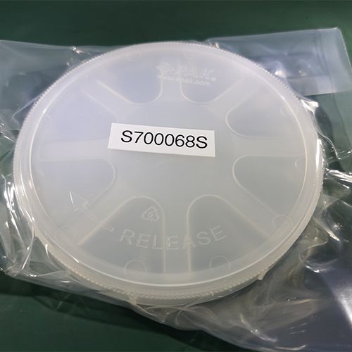
| Packaging Details: | single wafer package in 100-grade cleaning room |
| Delivery Time: | 2-4weeks |
| Payment Terms: | T/T, Western Union, MoneyGram |
| Supply Ability: | 5000pcs/month |
Product Description
2inch 4/6inch dia50.6mm sic seed wafer 1mm thickness for ingot growth
Customzied size/2inch/3inch/4inch/6inch 6H-N/4H-SEMI/ 4H-N SIC ingots/High purity 4H-N 4inch 6inch dia 150mm silicon carbide single crystal (sic) substrates wafersS/ Customzied as-cut sic wafers production 4inch grade 4H-N 1.5mm SIC Wafers for seed crystal
6inch SIC Wafer 4H-N Type production grade sic epitaxial wafers GaN layer on sic
Regarding Silicon Carbide(SiC) Crystal
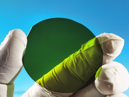
Silicon carbide (SiC), also known as carborundum, is a semiconductor containing silicon and carbon with chemical formula SiC. SiC is used in semiconductor electronics devices that operate at high temperatures or high voltages, or both.SiC is also one of the important LED components, it is a popular substrate for growing GaN devices, and it also serves as a heat spreader in high-power LEDs.
SiC Application
1 high frequency and high power electronic devices Schottky diodes, JFET, BJT, PiN,
diodes, IGBT, MOSFET
2 optoelectronic devices: mainly used in GaN/SiC blue LED substrate material (GaN/SiC) LED
Detail Information
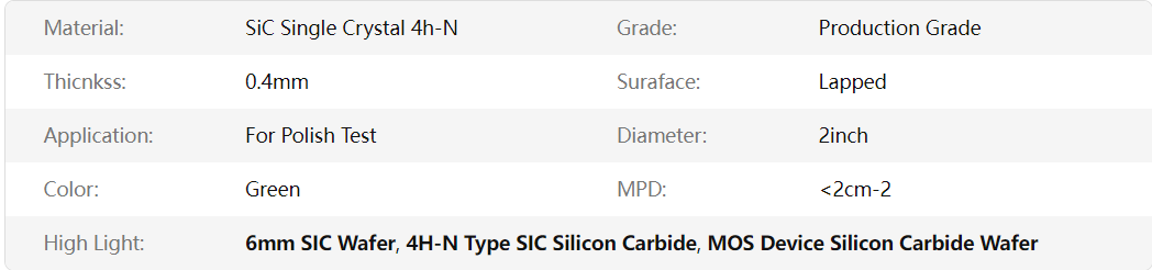
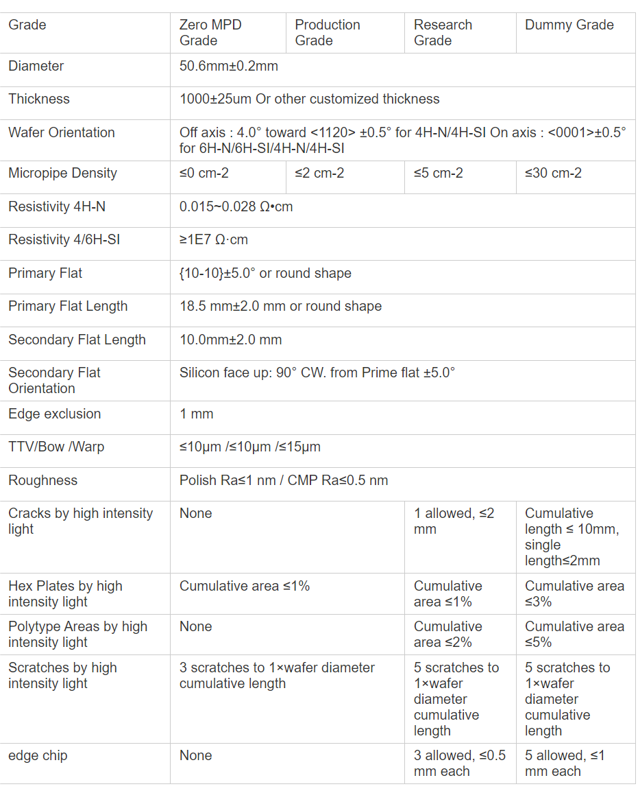
2inch diameter silicon Carbide(SiC) Substrate Speicfication
SiC ApplicationCatalohue Common Size In our Stock
| 4H-N Type / High Purity SiC wafer/ingots2 inch 4H N-Type SiC wafer/ingots 3 inch 4H N-Type SiC wafer 4 inch 4H N-Type SiC wafer/ingots 6 inch 4H N-Type SiC wafer/ingots | 4H Semi-insulating / High Purity SiC wafer2 inch 4H Semi-insulating SiC wafer 3 inch 4H Semi-insulating SiC wafer 4 inch 4H Semi-insulating SiC wafer 6 inch 4H Semi-insulating SiC wafer |
| 6H N-Type SiC wafer 2 inch 6H N-Type SiC wafer/ingot | Customzied size for 2-6inch |
We specialize in processing a variety of materials into wafers, substrates and customized optical glass parts.components widely used in electronics, optics, optoelectronics and many other fields. We also have been working closely with many domestic and oversea universities, research institutions and companies, provide customized products and services for their R&D projects.
It’s our vision to maintaining a good relationship of cooperation with our all customers by our good reputations.
Q: What’s the way of shipping and cost?
(1) We accept DHL, Fedex, TNT, UPS, EMS, SF and etc.
(2) If you have your own express account, it’s great.
Q: How to pay?
(1) T/T, PayPal, West Union, MoneyGram and
Assurance payment on Alibaba and etc..
(2) Bank Fee: West Union≤USD1000.00),
T/T -: over 1000usd ,please by t/t
Q: What’s the deliver time?
(1) For inventory: the delivery time is 5 workdays.
(2) For customized products: the delivery time is 7 to 25 workdays. According to the quantity.
Q: Can I customize the products based on my need?
Yes, we can customize the material, specifications and optical coating for your optical components based on your needs.